Electron Backscatter Diffraction (EBSD), when coupled with Scanning Electron Microscopy (SEM), is a powerful technique for characterizing the crystallographic structure of materials at the microscale. EBSD enables the determination of grain orientation, phase identification, and the analysis of microstructural features such as grain boundaries, twin boundaries, and texture. During analysis, a stationary electron beam interacts with a tilted crystalline sample, producing backscattered electrons that generate distinct diffraction patterns (Kikuchi patterns). These patterns are captured by a sensitive detector and analyzed to map crystallographic information with high spatial resolution. SEM-EBSD is widely used in materials science, metallurgy, geology, and semiconductor research for understanding structure–property relationships in polycrystalline materials.
Principle
Principle
The principle of EBSD in SEM is based on the diffraction of backscattered electrons from a crystalline sample. When a focused electron beam in the SEM strikes a tilted crystalline surface (typically at 70° to the horizontal), some of the incident electrons are scattered back out of the sample. A small fraction of these electrons undergo coherent elastic scattering within the crystal lattice, forming a diffraction pattern known as a Kikuchi pattern. This pattern is collected by a phosphor screen and recorded by a CCD or CMOS camera. By analyzing the geometry and intensity of the Kikuchi bands, the orientation of the crystal lattice at the beam interaction point can be determined. By scanning the beam across the sample surface, a map of crystallographic orientations and phases can be created, providing detailed insight into the material's microstructure.
Samples must have a flat, clean, and highly polished surface. For best results, final polishing with colloidal silica or ion milling is recommended. Conductive coating may be necessary for non-conductive materials.
EBSD can typically resolve grain sizes down to ~20–50 nm using advanced field emission SEMs, though resolution depends on material type, detector quality, and surface preparation.
Yes, EBSD can identify different crystalline phases based on their unique diffraction patterns, provided they have known structures in the EBSD database.
EBSD is a non-destructive technique in general, but prolonged exposure to the electron beam may cause local heating or slight damage, especially in sensitive or beam-unstable materials.
Applicable industries
Applicable Material Types
Metal Materials: Includes steels, aluminum, titanium, copper, and nickel-based superalloys, commonly analyzed for grain orientation and phase transformation.
Alloys: High-temperature alloys, stainless steels, and lightweight aluminum alloys benefit from EBSD's ability to assess microstructural integrity.
Composite Materials: Carbon fiber and glass fiber composites, where EBSD can study crystalline phases in embedded particles or interfacial behavior.
Ceramics: Technical ceramics such as alumina, zirconia, and silicon nitride, often used in harsh environments and examined for grain growth and orientation.
Semiconductors: Materials like silicon, GaN, and SiC, where crystal defects and orientation play a critical role in performance.
Rocks and Geological Samples: Granite, basalt, and limestone, studied to understand deformation mechanisms and mineral texture in earth sciences.
Biomaterials: Bone and dental materials, where EBSD provides insight into biological crystal structures like hydroxyapatite.
Industrial Application
Industrial Application
Aerospace: Used for analyzing turbine blades, engine components, and heat shields to assess grain orientation, phase stability, and failure mechanisms in extreme environments.
Automotive Industry: Helps evaluate steel and aluminum parts (e.g., gears, crankshafts, chassis) for texture and microstructural evolution after forming or welding.
Energy and Power: In nuclear and renewable energy sectors, EBSD is applied to study creep, grain boundary character, and irradiation effects in reactor components and turbine materials.
Construction and Infrastructure: Assists in analyzing steel reinforcements, welds, and concrete inclusions for structural integrity and phase transitions.
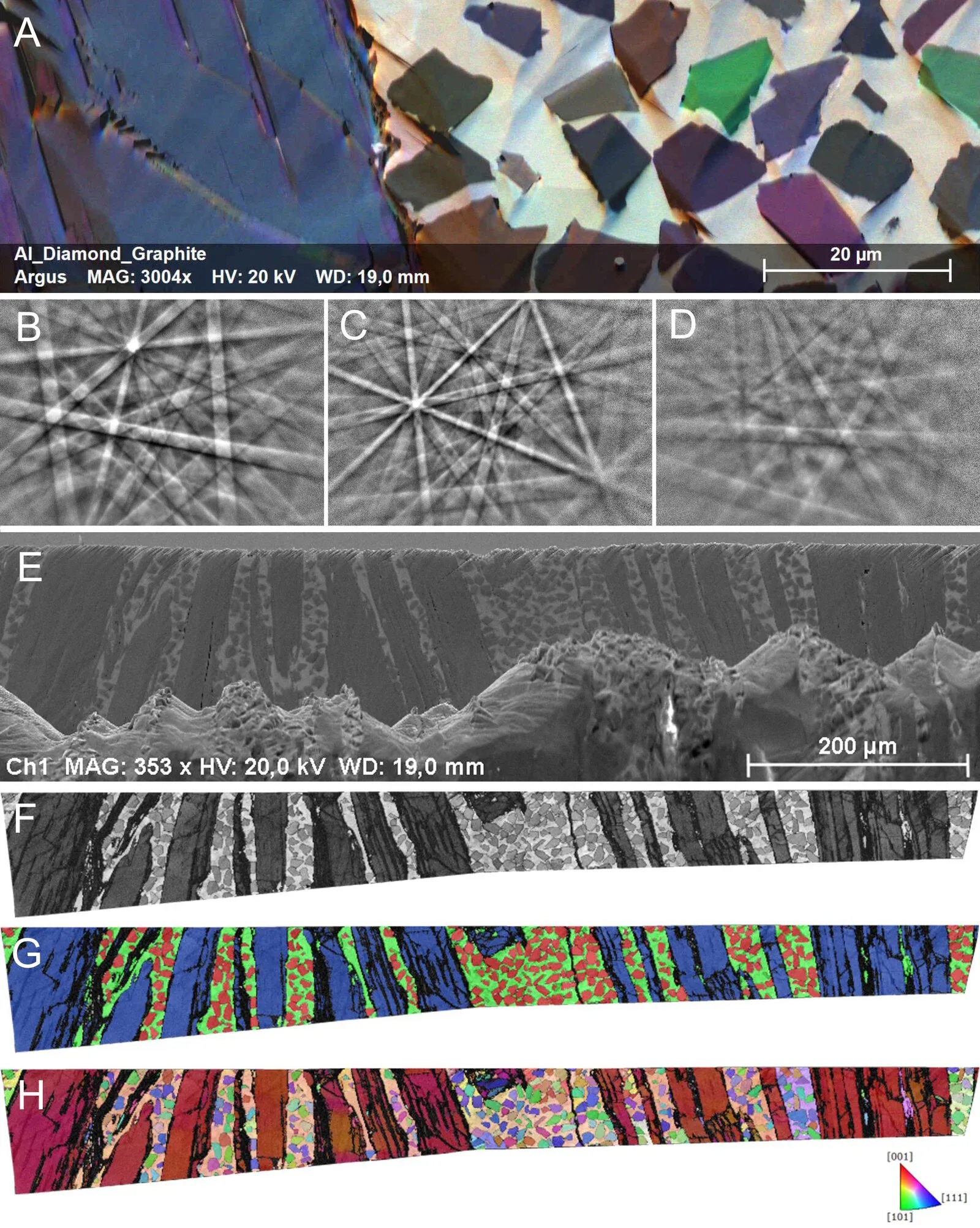
Caption: a) ARGUS FSE/BSE image after preparation using EM TXP and EM TIC 3X. EBSD patterns of the b) diamond, c) Al, and d) graphite phase. e) SEM image (taken with secondary electrons) showing an overview of the prepared surface which has a total size of 3 mm. f) Pattern quality map of the EBSD/EDS analysis. g) EBSD phase map showing the high indexing rate, even on the graphite flakes, where graphite is displayed in blue, diamond in red, and Al in green. h) Corresponding IPF-X / EBSD orientation map along the X axis.
Technical Parameters
Flat and Smooth Surface: The sample surface must be well-polished to produce high-quality Kikuchi patterns. Mechanical polishing followed by electro-polishing or ion beam polishing is often required.
Crystalline Structure: EBSD only works on crystalline materials; amorphous materials do not produce diffraction patterns.
Tilt Angle: The sample must be mounted at a ~70° tilt relative to the electron beam to optimize backscatter electron detection.
Size and Thickness: Samples should fit into the SEM chamber and typically be less than a few centimeters in size. Cross-sections should be thin enough if using in situ setups.
Conductivity: Non-conductive materials (e.g., ceramics, polymers, geological samples) may require a thin conductive coating (e.g., carbon or gold) to prevent charging.
Cleanliness: Surface should be free from contamination, oxidation, or debris to avoid interference with the diffraction signal.
Military and Defense: Used in armor materials, ballistic components, and aerospace-grade alloys to ensure reliability and resistance to dynamic loading.
Electronics and Semiconductors: Critical in microelectronics for mapping defects, studying thin film texture, and improving crystal growth processes.
Biomedical Engineering: Applied to metallic implants and bio-ceramics to assess grain structure and phase distribution, improving mechanical compatibility with human tissue.
SEM EBSD (Scanning Electron Microscopy with Electron Backscatter Diffraction) is a microstructural analysis technique used to characterize the crystal orientation, phase distribution, and grain boundaries of materials. It works by detecting diffraction patterns generated by backscattered electrons to reveal detailed crystallographic information.