Scanning Electron Microscopy (SEM) is an advanced imaging technique that uses a focused beam of high-energy electrons to scan and analyze the surface of a sample. The interaction between the electron beam and the sample generates signals (secondary electrons, backscattered electrons, and X-rays), which are detected to create detailed images and provide information about the sample’s surface morphology, structure, and composition.
Key Features
High Resolution: SEM provides high-resolution imaging, typically ranging from 1 to 10 nanometers.
Surface and Elemental Analysis: It reveals detailed surface topography and, with additional tools like Energy Dispersive X-ray Spectroscopy (EDS), can also provide elemental composition.
Wide Applications: SEM is used in materials science, nanotechnology, biology, and electronics for studying surfaces, microstructures, and composition.
Principle
Principle
Electron Beam Generation:
Electrons are emitted from an electron gun (either thermionic or field emission).
The electron beam is accelerated (typically 0.5–30 keV) and focused into a fine probe using electromagnetic lenses.
Scanning the Surface:
The focused beam scans over the sample in a raster pattern (line by line).
As the beam interacts with the atoms at or near the surface, various signals are generated.
Signal Generation:
Key signals produced include:
Secondary Electrons (SE): For surface morphology (high-resolution imaging).
Backscattered Electrons (BSE): For atomic number contrast.
Characteristic X-rays: For elemental analysis (via EDS/EDX).
Auger electrons: Used for surface chemistry in some modes.
Electron beam-induced current (EBIC) and other effects in specialized modes.
Yes, SEM generally requires samples to be conductive to prevent electron beam buildup on the surface, which can affect image quality. Non-conductive samples (such as plastics or biological samples) usually need to be coated with a metal layer (like gold or platinum) to improve conductivity.
The electron beam used in SEM can cause some damage to sensitive samples, especially organic or biological materials. Therefore, it's important to use low electron beam currents and voltage to minimize damage. For very delicate samples, techniques such as cryo-SEM (freezing) can be used to reduce the impact.
SEM primarily analyzes the surface structure of samples. To investigate internal structures, samples may need to be sectioned, fractured, or complementary techniques such as Transmission Electron Microscopy (TEM) may be used.
SEM typically provides a resolution of 1-10 nanometers, and in some cases, even higher. This enables the observation of fine details such as nanoparticles, surface cracks, and other microstructures.
Applicable industries
Applicable materials type
Metal Materials: Fracture analysis, corrosion studies, alloy microstructure analysis.
Pharmaceutical and Food Industries: Drug particle morphology, food microstructure analysis.
Nanotechnology: Surface morphology and structural analysis of nanomaterials and devices.
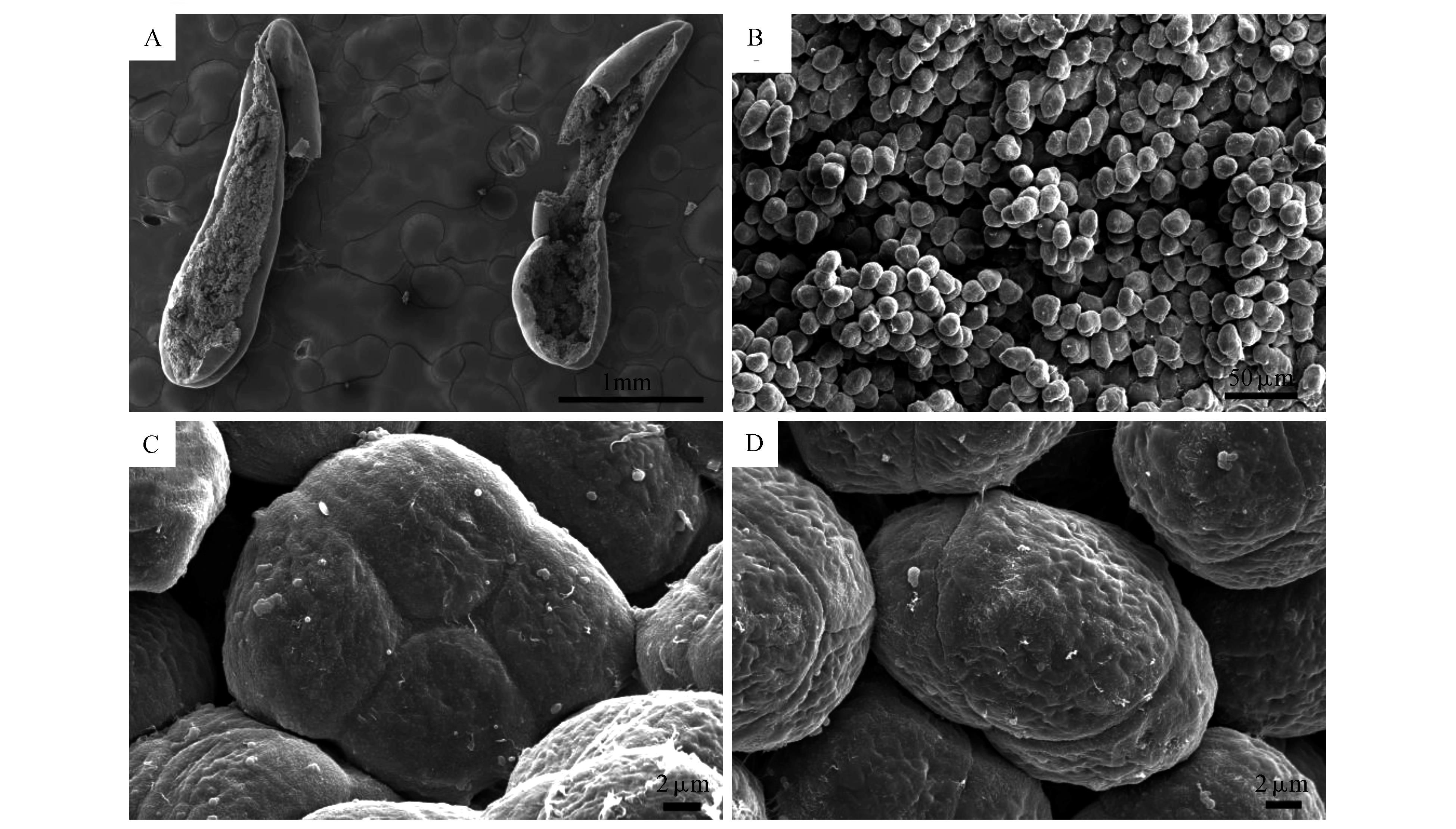
Caption: Pollen Microstructure Observation
Principle
Sample Conductivity: SEM needs conductive samples.Non-conductive materials (e.g., ceramics, plastics, bio-samples) should be coated with a thin metal layer (like gold or platinum) to avoid charging and image distortion.
Sample Size: The sample must fit inside the SEM chamber (usually a few centimeters).Oversized samples may need trimming or adjustment.
Sample Stability: The sample should stay stable under the electron beam.Heat- or beam-sensitive materials (like organics or biological samples) may require cryo-treatment.
Sample Vacuum Compatibility:SEM works in high vacuum.Moist or volatile samples need dehydration, freeze-drying, or other protective methods to remain stable.
Sample Chemical Composition: Materials with high atomic numbers (e.g., metals) produce stronger signals and better images.For complex samples, EDS (Energy Dispersive X-ray Spectroscopy) can be used for element analysis.
Sample Cleanliness:The sample surface should be clean.Contaminants can cause unwanted signals and affect image quality.
Detection and Image Formation:
Signals are collected by appropriate detectors (e.g., Everhart–Thornley detector for SE).
The intensity of the signal at each scanned point is mapped to brightness in the final image.
Scanning Electron Microscopy (SEM) morphology imaging is a high-resolution technique used to observe the microstructure and surface features of materials. By focusing an electron beam on the sample surface and collecting the resulting secondary electron signals, SEM produces clear images with nanometer-scale resolution, revealing surface roughness, particle shape, pore distribution, and fine surface textures.